ECE425 Analysis and Design of Analog IC - Operational Amplifier Design (Fall2015)
Introduction
In this project, we are asked to design an Operational Amplifier with some specific requirements. The operational amplifier is a theoretical component that should have infinity input impedance and zero output impedance. At the same time, it should have infinity open-loop gain. One can do a lot of designs such as filter, adder, multiplier with Operational Amplifier. But in the real world, the operational amplifier will never be theoretical since all the parameters cannot go to zero or infinity.
I designed a two-stage CMOS Opamp (Operational Amplifier) with 65 ns Technology in this project. The schematic of the design can be shown in Figure 1.
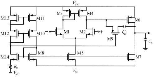
Figure 1. Two stage CMOS Opamp.
Compare to conventional Opamp, this kind of schematic has a robust bias circuit (including M8 and M10 – M14), which will offer a very stable ID5 compare to a single resister. In the middle stage is a standard NMOS differential amplifier. The top M3 and M4 is a typical current mirror, and this current mirror will split ID5 and make sure M1 and M2 are in working mode. The WL ratio of M3 and M4 will mainly affect the input common-mode range. M1 and M2 are the main amplifier transistor at this level. Different M1 M2 will give us different Gain Bandwidth. M5 is the pull-down circuit, with the help of the bias circuit, it can offer a known ID5 to the differential amplifier. Stage 3, including M6 and M7 is an output buffer. M6 is working as a Common Source amplifier. Together with M1 and M2, it can give us around 60 DC gain. M9 and Cc is the compensation feedback component. Different M9 and Cc will give us different Phase margin and bandwidth. The design procedure of all these components will be included in detail in the following section.
While I was designing the amplifier, I found many limitations of Opamp. And also, I found some efficient design methods by working with MATLAB and Microsoft EXCEL.
Calculations
In order to calculate the frequency and gain response, one need small-signal equivalent circuit. Figure 2 shows the small signal equivalent circuit of the CMOS Opamp in Figure 1.
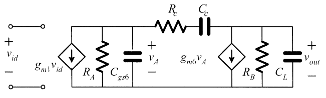
Figure 2. Small signal equivalent circuit.
By listing the KCL and KVL of the small signal equivalent circuit, we can know the transfer function of the circuit.
\(\frac{V_{A}}{\frac{1}{S C_{1}}}+\frac{V_{A}}{R_{A}}+g_{m 1} V_{i d}+\frac{V_{A}-V_{o u t}}{\frac{1}{S C_{c}}}=0\)
\(V_{o u t}\left[s\left(C_{L}+C_{c}\right)+R_{B}\right]=V_{A}\left(s C_{c}-g_{m 2}\right)\)
We can derive the transfer function from these two equations.
\(\frac{V_{\text {out}}}{V_{\text {in}}}=\frac{g_{m 1} R_{A} g_{m 2} R_{B}\left(1-\frac{S C_{C}}{g_{m 2}}\right)}{s^{2}\left\{R_{A} R_{B}\left(C_{1} C_{2}+C_{1} C_{c}+C_{2} C_{c}\right)+s\left[R_{A}\left(C_{c}+C_{2}\right)+R_{A}\left(C_{c}+C_{2}\right)+C_{c} g_{m 2} R_{A} R_{B}\right]+1\right.}\)
Compare to the standard two stage Opamp transfer function. We can know the poles and zeros of the Opamp.
\(Z=\frac{g_{m 2}}{C_{c}}\)
\(P_{1}=\frac{1}{g_{m 2} R_{A} R_{B} C_{c}}\)
\(P_{2}=\frac{g_{m 2}}{C_{c}}\)
\(A_{d c}=g_{m 1} R_{A} g_{m 2} R_{B}\)
After knowing these very important equations of an Opamp circuit, we can start to calculate the parameters of the components in our circuit. Following is the most useful equations while I do the calculation.
\(I_{D}=\frac{\mu_{n, p} C_{\mathrm{ox}}}{2}\left(\frac{W}{L}\right) V_{\mathrm{eff}}^{2}\)
\(g_{m}=\sqrt{2 \mu_{n, p} C_{\mathrm{ox}}\left(\frac{W}{L}\right) I_{D}}\)
\(g_{m}=\frac{2 I_{D}}{V_{\mathrm{eff}}}\)
Before I do further calculation, I list all the specifications from the final project manual as follow.
Transfer function shape: Open loop gain > 500 First order low-pass filter behavior for open loop transfer function. Feedback factor as determined by the circuit in Fig. 1. Loop transmission unity gain frequency > 5MHz (Resulting open loop unity gain frequency > 50MHz) Phase margin > 60° (open loop) Gain margin > 2 (open loop)
Slew rate > ± 20V/μs
Input common mode range: 0.3V to 0.9V
Input offset voltage < 5mV
Output swing range: 0.3V to 0.9V
Starting from gain bandwidth, according to the definition we know that
\(G B W=A_{d c} P_{1}=\frac{g_{m 1}}{C_{c}}\)
So, the Gain Bandwidth product is mainly correlated to M1 M2 and Cc these three components. Let’s decide what value we want for Cc first. We can easily know that the dominant load capacitance in the circuit is the load capacitance which is 10 pF as it is specified. In the requirement, Phase Margin (PM) of the amplifier have to be larger than 60 degree (deg). In order to achieve 60 deg PM, the following equation have to be satisfied.
\(P M=84.29 \operatorname{deg}-\tan ^{-1}\left(\frac{G B W}{P_{2}}\right)\)
After calculation, we know that we have to make Cc larger or equal than 0.22*CL. To get make sure that the PM will be satisfied for sure, I make Cc = 3 pF.
According to SR=I_5/C_c, we know that I_5=SRC_c=20 V/us*3 pF=60 uA . So I need to design ID5 as 60 uA to make sure SR is larger than 60 deg.
The following equation determine the required gm1 value to assure the GBW.
\(g_{m 1}=G B W * C_{c} * 2 * p i=50 M * 3 p F * 2 * p i=942.4 u\)
Knowing gm1 and ID5, I can finally calculate the Width by Length ratio (WL ratio). ID1 and ID2 is ID5/2 because of the current mirror.
\(\left(\frac{W}{L}\right)_{1,2}=\frac{g_{m 1}}{u n C o x * 2 * I D 1} \approx 49.348\)
unCox and upCox are the most common values in the CMOS design. By checking the 65ns technology manual, we can easily know that for the transistor we are using in the system
\(u n C o x=300 u A / V^{2}\)
\(u p \operatorname{Cox}=110 u A / V^{2}\)
Input Common mode range is specified as 0.3V to 0.9V. M3 and M4 will affect the ICMR(+). ICMR(+)=0.9V. ICMR(-)=0.3V. To put all the devices in saturation mode, the following formula need to be satisfied.
\(\operatorname{ICMR}(+) \leq\left[V D D-\left(\sqrt{\frac{2 I_{D}}{\beta}}+\left|V_{t 3}\right|\right)\right]_{\min }+V_{\operatorname{timin}}\)
So that we know that WL ratio of M3 and M4 are
\(\left(\frac{W}{L}\right)_{3,4}=\frac{2 * I_{D 3}}{u p C o x\left[V D D-I C M R(+)-V_{t 3 m a x}+V_{t 1 m i n}\right]^{2}}=5.5676\)
\(V_{t 3 m a x}=0.294 V\)
\(V_{t 1 \min }=0.307 V\)
Vt3max and Vt1min are obtained by DC simulation in the testbench as follow.
To design M5, we need to derive it from ICMR(-).
\(V_{D S A T} \geq I C M R(-)-\sqrt{\frac{2 I_{D}}{\beta}}-V_{t 1 \max }\)
Since my design have the input stage as NMOS transistors, so when ICMR(-) is less than 0.5, I will get a negative VDSAT which is impossible. So I decided to make the ICMR(-) as large as possible. I have to make the VDSAT large enough to make the amplifier work, and I want a decent ICMR(-). I decided to make ICMR(-) equal to 0.5 other than 0.3.
Ps: I know ICMR(-)=0.5 doesn’t meet the requirement, and I know the solution is to use the complementary input stage. However, I tried my best testing the circuit coming from some other papers, it just doesn’t work. I even have my PMOS version of two stage amplifier design and it also works fine. But the PMOS Opamp have a ICMR(+) less than 0.6. I do have the complementary schematic design in the Final folder, but I failed to test it. This ICMR(-) is the only part that doesn’t meet the requirement.
Using ICMR(-)=0.5V, I know that the VDSAT =165.3 mV
\(\left(\frac{W}{L}\right)_{5,8}=\frac{2 * I_{D 5}}{u n \operatorname{Cox} V_{D S A T}^{2}}=6.22\)
In order to have a PM larger than 60 deg, we need to make gm6 >= 10 gm1. Use gm6=10gm1=9.4248m. We know that
\(\left(\frac{W}{L}\right)_{6}=\frac{g_{m 6}}{g_{m 4}}\left(\frac{W}{L}\right)_{4}=273.734\)
ID6 and ID7 are the same, by this relation we can get
\(I 6=I 7=\frac{\left(\frac{W}{L}\right)_{6}}{\left(\frac{W}{L}\right)_{6}} * \frac{I 5}{2}\)
\(\left(\frac{W}{L}\right)_{7}=\frac{I_{7}}{I_{5}}\left(\frac{W}{L}\right)_{5}=359.7069\)
As for M10-M14 and Rb these are to give a proper Vbias to have a 60 uA ID5. These values are not that critical and also it is very easy to calculate it. Any value that make ID5 =60uA will be fine.
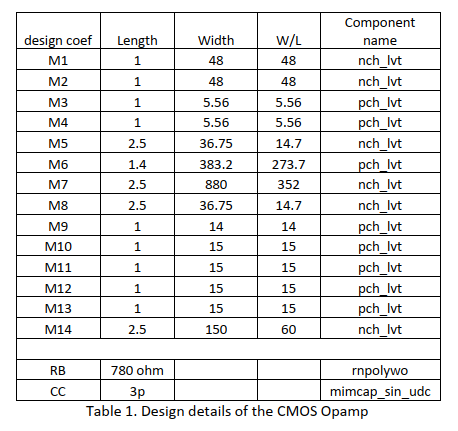
Till now we have the parameters of all the components in the circuit calculated. These parameters can be shown in Table 1.
All the calculation is done by using MATLAB. I wrote a script in Matlab to finish the calculation. The matlab code can be shown in the following context:
%in version 1.1 i change the uncox and upcox
clear;
clc;
GBW = 50 * 10^6;    %gain band width == 50 MHz
SR = 20 * 10^6;     %slew rate == 20V/us
DC_GAIN = 500;      %open loop gain == 500
PM=60/180*pi;
GM = 2;             %gain margin
VDD = 1.2;          %VDD == 1.2V
VSS = 0;            %VSS ==0 Grounded
ICMRp = 0.9;
ICMRm = 0.6;
Cl = 10 * 10^-12;

%uncox = 2 * (22 * 10^-6) * ((130 * 10^-9)/(650 * 10^-9)) * 1/(703.3*10^-3 - 561.2*10^-3)^2;
%upcox = 2 * (22 * 10^-6) * ((130 * 10^-9)/(650 * 10^-9)) * 1/(-729.5*10^-3 + 492.9*10^-3)^2;
unCox = 300 * 10^-6;
upCox = 110 * 10^-6;
%unCox = 318.4 * 10^-6;
%upCox = 149.2 * 10^-6;
Cox = 19 * 10^-15 / 10^-12;
up = upCox / Cox;
un = unCox / Cox;
WL(8)=0;            %WL ratio to be calculated

Lmin = 500;

Cc = 0.3 * Cl;  %1.83 is a fix
I5 = SR * Cc;     %1.3 is a fix
gm1 = GBW * Cc * 2 * pi; %1.06 is a fix
WL(1) = gm1^2/(unCox * I5); %wl 1
WL(2) = WL(1);
vt3max = 0.294; vt1min = 0.307;   %obtained by simulation
WL(3)= I5 / (upCox*(VDD-ICMRp-vt3max+vt1min)^2);
WL(4)=WL(3);
vt1max = 0.371;
VDSAT5 = ICMRm - sqrt(I5/(WL(1)* unCox)) - vt1max; %6 should be WL1

WL(5) = 2*I5/(unCox*VDSAT5*VDSAT5);
WL(8) = WL(5);
gm6 = 10*gm1;
gm4 = sqrt(upCox* WL(4)*I5);
WL(6) = gm6/gm4 *WL(4);
L6=sqrt(3*up*0.3*Cc/(2*GBW*2*pi*(Cc+Cl) * tan(PM)));

I6 = WL(6)/WL(4)* I5/2;
I7=I6;
WL(7)= I7 / I5 * WL(5);
WL(9)=2*Cc*SR/(upCox*0.3*(VDD-0.3-2*0.3));
RB=1/(sqrt(2*unCox*WL(8)*Cc*SR));
WL(10) =WL(6)*WL(8)/WL(7);
WL(11) =WL(10);
WL(12) =WL(11);
WL(13) =WL(12);
WL(14) =4*WL(8);

P=SR*(3*Cc+Cl)*(VDD-VSS)
WL
Schematics and Simulations
Schematic Setup
Figure 3 shows the schematic of the CMOS Opamp design. This schematic is while I was doing the system setup.
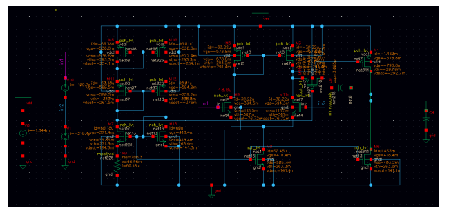
Figure 3. Schematic of two stage Opamp.
After finishing the design, I pack the amplifier and form a symbol view of the Opamp. The design schematic and symbol can be shown in Figure 4.
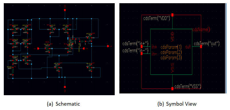
Figure 3. Opamp Schematic and Symbol View.
Bode Plot (DC gain & Unity Gain Frequency & Gain Margin)
In figure 1, it also shows the DC operating points of all the components, these values will also be included in on single table in the performance evaluation section. ICMR is from 0.5 to 0.9, So by using AC analysis scanning from 10 Hz to 10 GHz, I can obtain the bode plot of the system by direct plot it in the result tab. I scheme the bode plot of open loop amplifier with load capacitance of 10 pF. The result can be shown in figure 5.
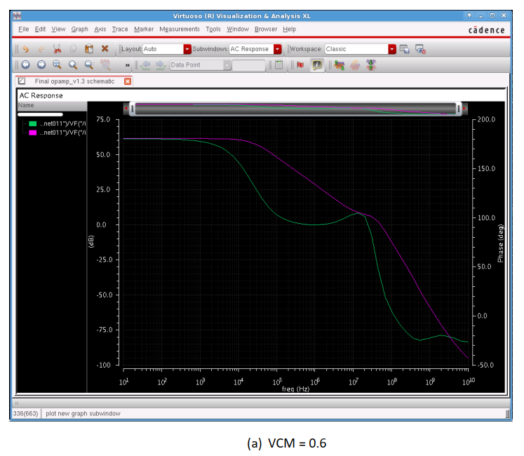
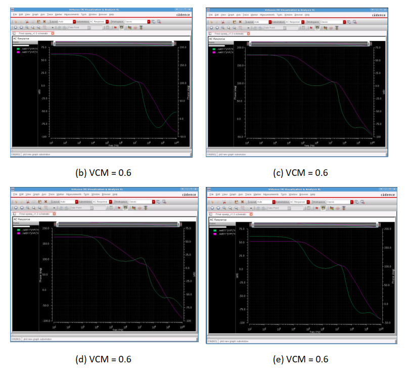
Figure 4. Bode Plot of the Openloop Circuit (10Hz - 10 GHz).
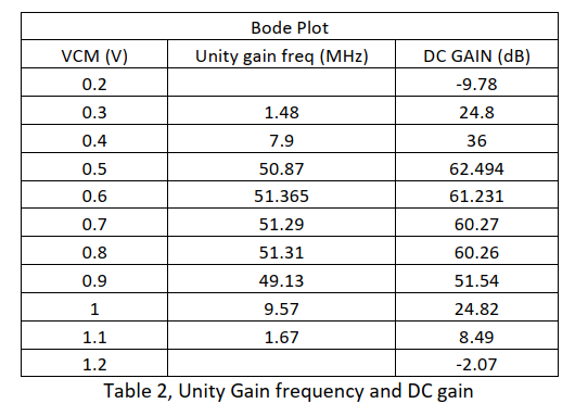
From the Bode plot we can easily know the unity Gain frequency and openloop DC gain. All the information are summarized in Table 2.
Gain margin can also be derived from the Bode plot. Gain margin is defined as the amount of gain increase or decrease required to make the loop gain unity at the frequency Wgm where the phase angle is –180° (modulo 360°). To make is simpler, it is the gain of the circuit while phase is equal to 180 deg. Gain margin is calculated using the following formula. It can be drawn from Bode plot in the following figure.
\(Gain margin$=1-\operatorname{Gain} @ 180^{\circ}$ phase shift\)
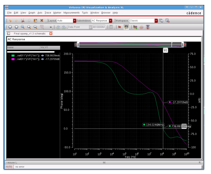
As it is shown in the figure, the Gain margin is -17.2970dB which is larger than 2, so it meet the requirement.
Phase Margin Test
Phase margin is defined as the phase shift at the frequency that gain equal to 1 which is 0 dB. To test the Phase margin, we need to analysis the Bode plot of the open loop circuit again. By putting the markers on the frequency axis and dB and phase axis, we can obtain the Phase margin of the circuit. Figure 5 shows the procedure of getting the Phase margin of the circuit.
As shown in figure 5, the phase margin is around 60 deg.
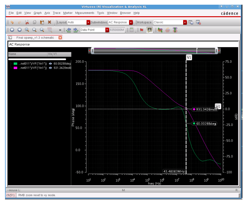
Figure 5. Phase Margin obtaining.
Slew Rate Test
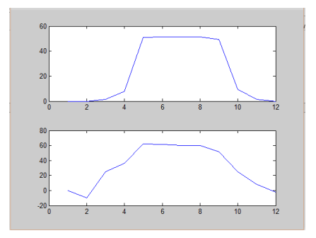
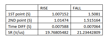
Slew Rate describe the voltage changing speed of the output. This directly affect the operating speed of the Opamp. The method of testing the Slew rate is to divide voltage changing rate by time. I decide to test the slew rate from %25 output to %75 output voltage. The testbench can be shown in Figure 7 and the slew rate for both rising edge and falling edge can be shown in Figure 8. The input voltage of the amplifier is a rectangular wave, this is to make the testing procedure easier.
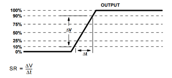
Figure 6. Slew Rate Testing Method.
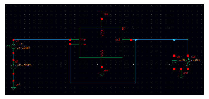
Figure 7. Slew Rate Testbench.
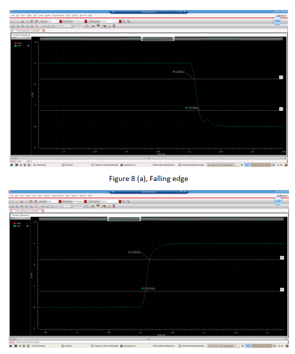
Figure 8. Rising edge and Falling edge.
Deriving from the testing, slew rate is calculated in Table 3. To make it easier, I use Excel to do the calculation. The Excel chart is also included in the design submission.
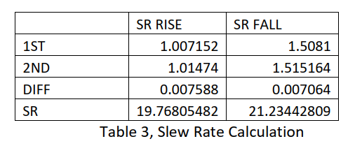
According to the table, the rising slew rate is 19.768 V/us and the falling slew rate is 21.234 V/us. So the slew rate basically meet the requirement.
Input offset Voltage
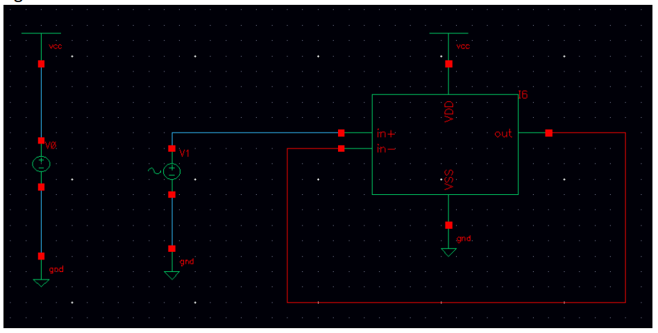
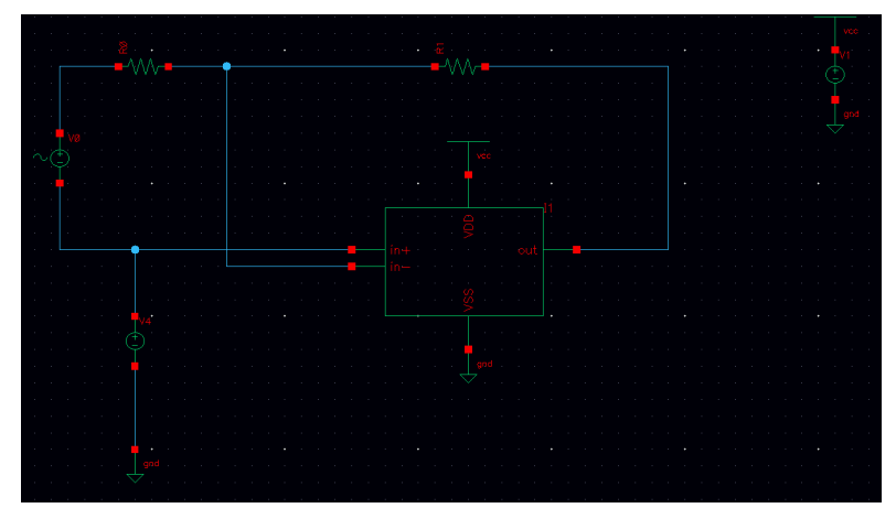
The input offset voltage of the amplifier is a parameter defining the differential DC voltage required between the inputs of an amplifier. It shows if the circuit is well balanced or not. The testbench can be shown in figure.
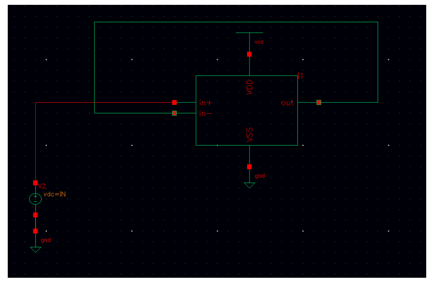
Figure 9. Input offset voltage Testbench.
In order to test the mismatch of the output voltage and input voltage, I scan the input voltage value from 0V to 1.2 V. The output and input voltage are shown in the following figure
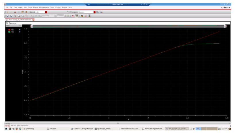
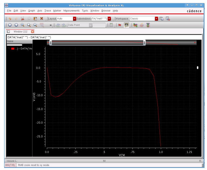
To make a better comparison, I use output voltage to minus input voltage and I get the result as it is shown in the following figure.
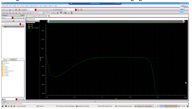
This figure can perfectly show the input offset voltage of the circuit. From 0 V, the output should also be 0 V. When the VCM goes to around 0.4V, the transistors start to be in saturation mode and gradually build the balance. When VCM = 0.5, the amplifier is in the working mode and till 0.9V, the input offset voltage is still less than 1 mV which is very nice.
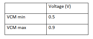
Input Common Mode Range
Input Common Mode Range (ICMR) is the voltage that can be applied to both input port to make the circuit in the correct working mode. With a proper input voltage, all the transistors should be in saturation mode. The following figure shows the test bench of ICMR.
Vin can’t be connected to ground as it is shown in the lab manual, that is because we have only one single power supply in the circuit. In order to test the VCM range, I scan the input voltage from 0V to 1.8 V. I am getting the output voltage as it is shown in the following figure
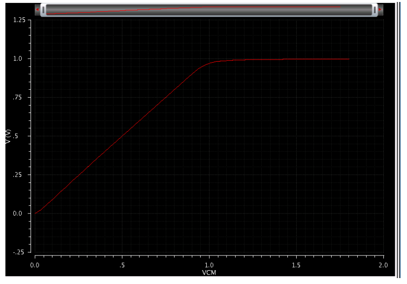
The input voltage VCM is a scan from 0 V to 1.8V. To view the result better, I did a subtraction to the input voltage and the output voltage by using calculator in the tool tab, the result can be shown in the following figure
It can be clearly seen that the voltage become stable at 0.5V and keep flat until 0.9V. I didn’t use the complementary input technology, so form 0.3 to 0.5 is not the proper VCM.
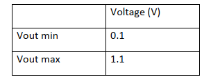
Output swing
The output swing is the range that the output can approach. The testbench of the output swing can be shown in the following figure.
To make this simpler, I make both R1 and R2 as 10K, so this schematic become an input follower. Whatever I have as the input the output will give up the same output. And I set the simulation at transfer function analysis. I tested a few set of input and found the output swing at around 0.1 to 1.1 which is larger than 0.3 to 0.9. The following figures shows the simulation results. Among all these test cases, the VCM is 0.6.
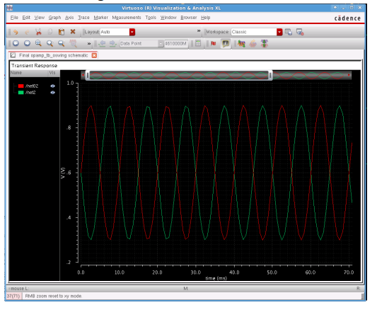
Openloop response
In order to see the performance of the output signal compare to the input signal. I select tran analysis and do the simulation. The VCM is set to 0.6 V. And input have a Vpp of 0.2mV and frequency of 10Hz. The following figure shows the plot of output signal and input signal. The input signal looks like a single line that is because the input swing is too small.
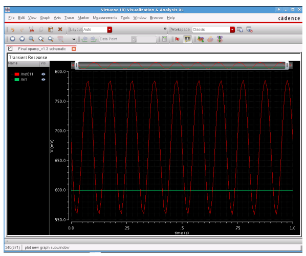
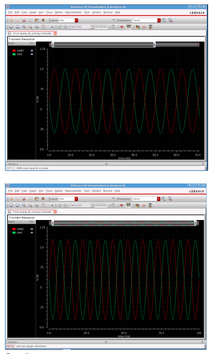
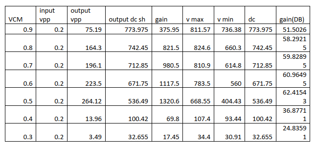
I also test the same setup with different VCM the output can be shown in the following Table.
Performance evaluation
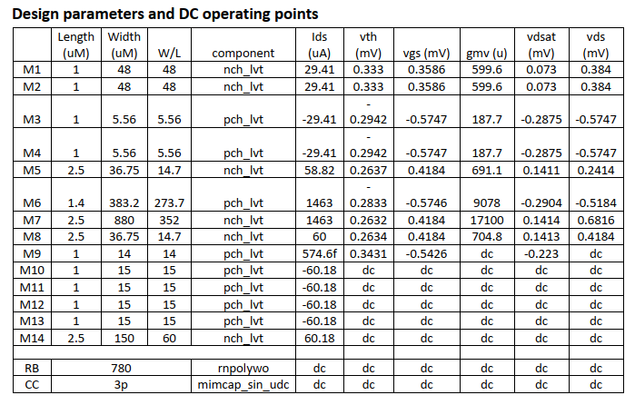
This table shows all the design parameters and their DC operating points. ‘dc’ in the table means ‘don’t care’, don’t care is not saying I didn’t carefully design them, it means these value are not critical to the design.
Openloop Gain
The following Table is drawn from the Bode Plot with different VCM.
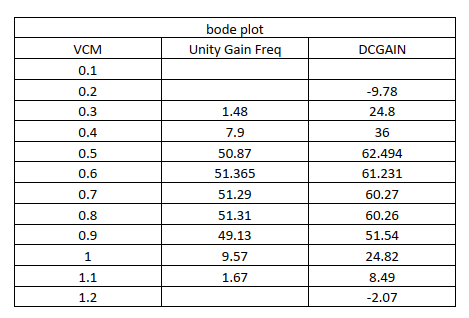
The upper figure is the unity gain Frequency, it is almost stable while VCM is 0.5V to 0.9V. The bottom figure is DC gain compare to the VCM.
Slew Rate
As it presented before, Slew rate is tested by dividing voltage change by time interval. The following table shows that rising slew rate is 19.768 V/us and falling slew rate is 21.234 V/us
ICMR
Output swing
Power Consumption
Although there is no requirement on the power consumption. I still did a static power consumption check for my design. The following figure is the result.
The static power consumption is 1.969 mW. According to my calculation, the power consumption is 0.456 mW. I think the additional power consumption are coming from the bias circuit, since I have added a lot more transistors to stabilize the ID5 to be 60 uA.
Conclusion
In the final project, I designed a two stages CMOS Opamp. The Opamp mainly has 3 parts, the first part is to generate a bias voltage for the coming two stages. This stage will stabilized the ID5 as 60 uA. The second stage is a differential amplifier which have a gain of around 30 dB. The third stage is a Common Source amplifier which have a gain of around 30 dB. My design has a ICMR of 0.5 to 0,9 V and output Swing as 0.1 to 1.1 V. All the project specifications are met except for ICMR is not from 0.3 to 0.9. That is because of the NMOS input stage. I tried to implement the complementary input stage with both NMOS and PMOS however it doesn’t really work as expected. Designing with MATLAB and EXCEL make life a lot easier since a lot of parameters need to be taken care of. All the projects including EXCEL sheet and MATLAB code and design file itself are included in the tar file.
Reference
[1] Design Procedure for Two-Stage CMOS Opamp With Flexible Noise-Power Balancing Scheme