WeekendPrj: Adapting OV7670 camera module with Nexys4 DDR board (2017)
Introduction
This is a one weekend hobby project I have done in Spring 2017. Most the codes are referenced from online, I would not re-upload the code in my github. I ll only described what I have done in this project. (Note: This is the first github project I have ever created. The project itself is simple and straight forward, all I want is to get familiar with Github and reStructuredText. Hopefully this is helpful for you if you are new to FPGA.)
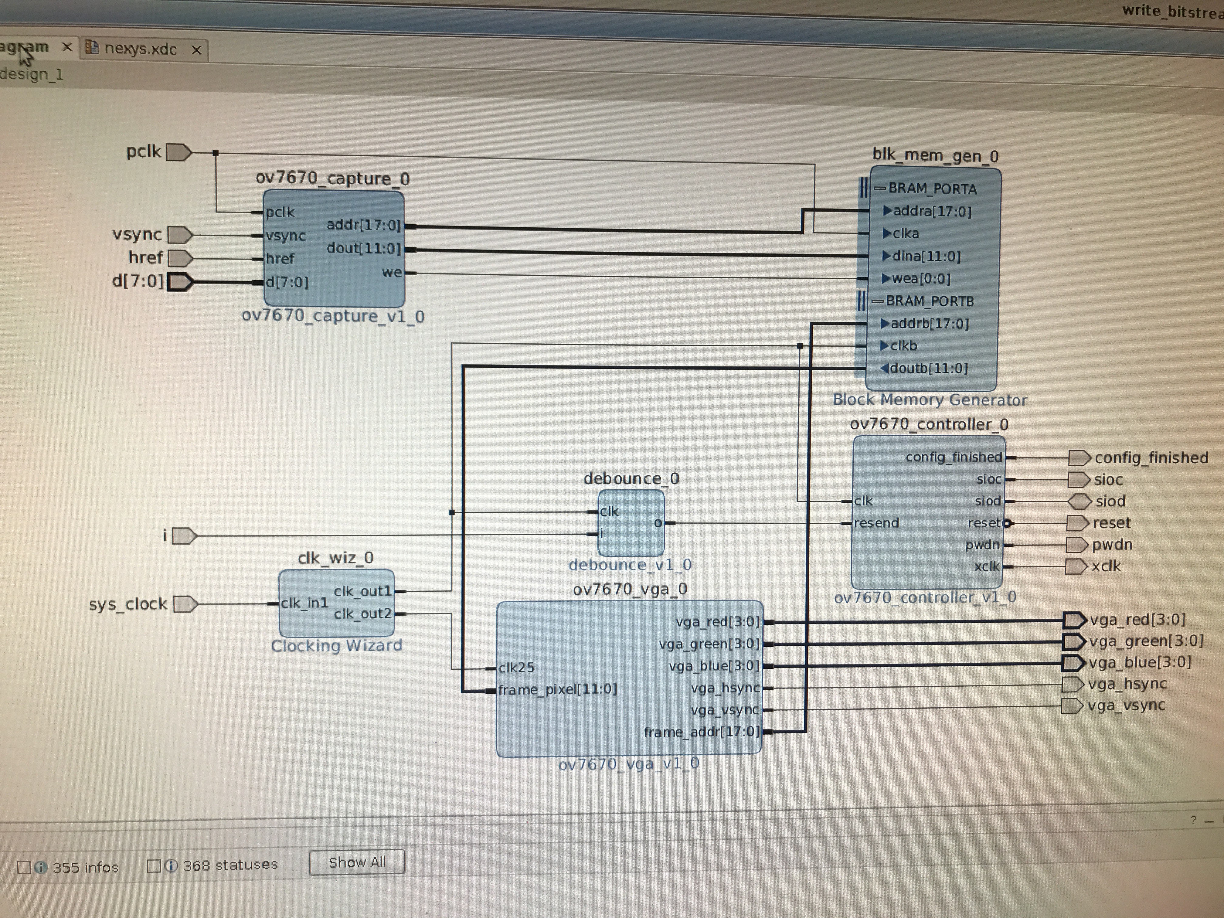
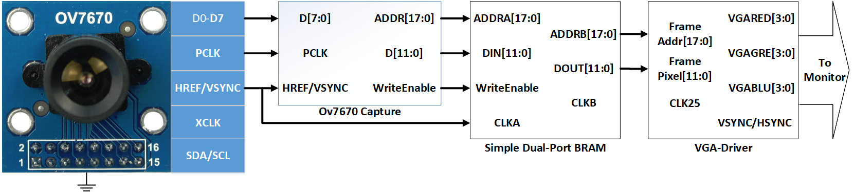
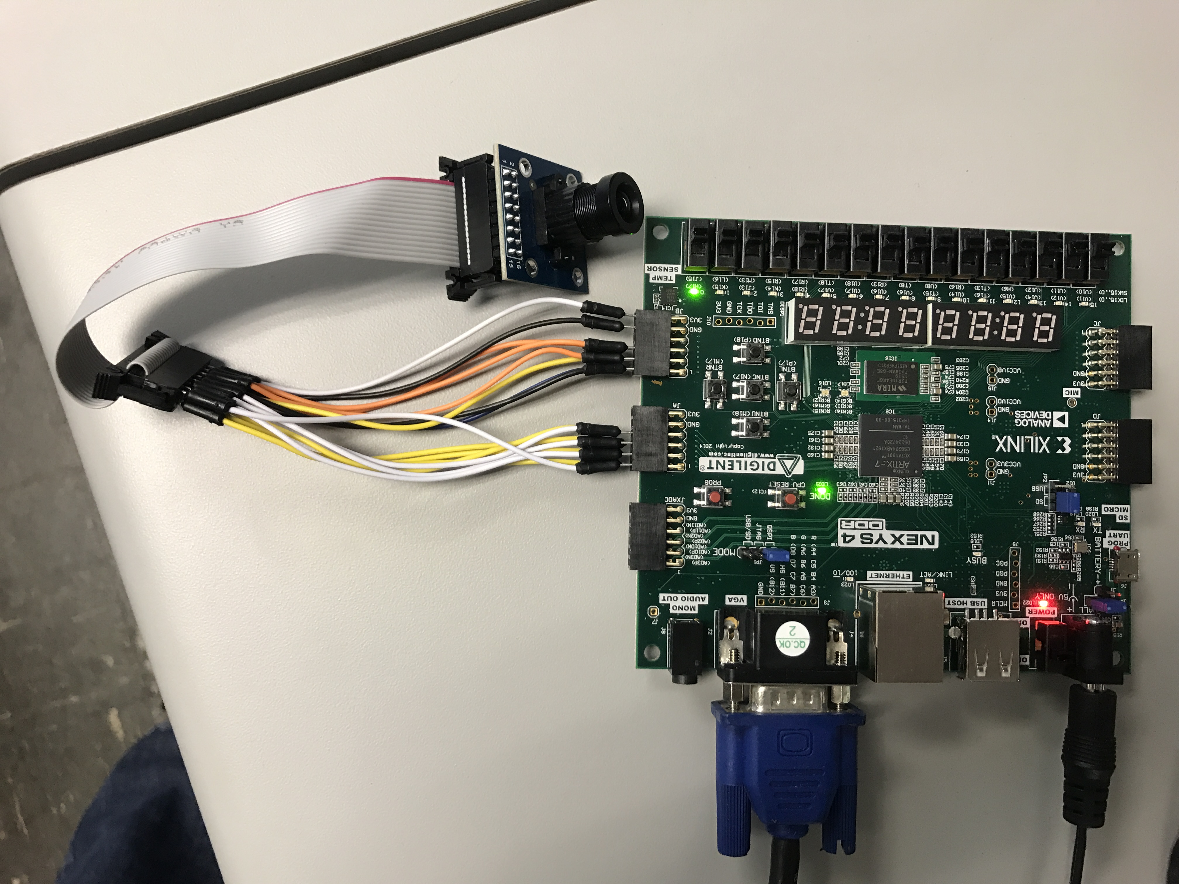
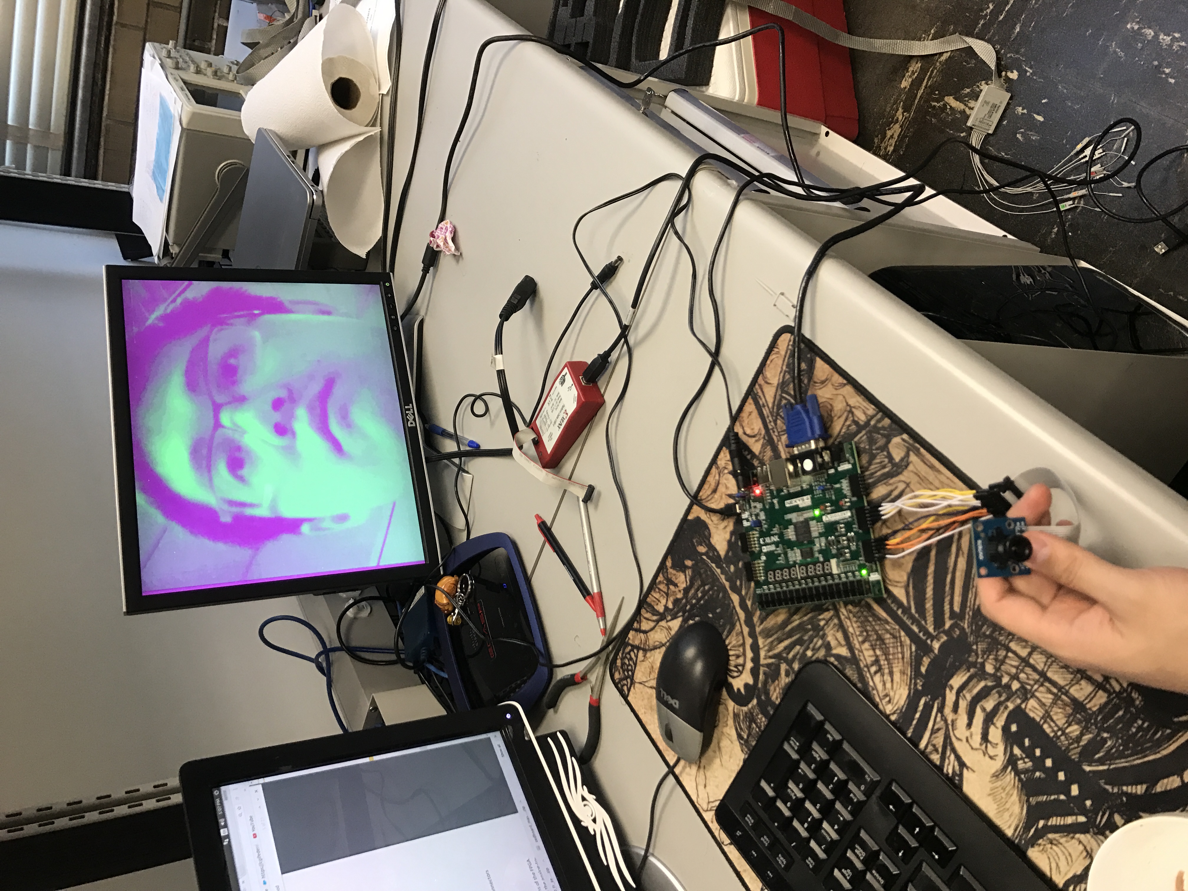
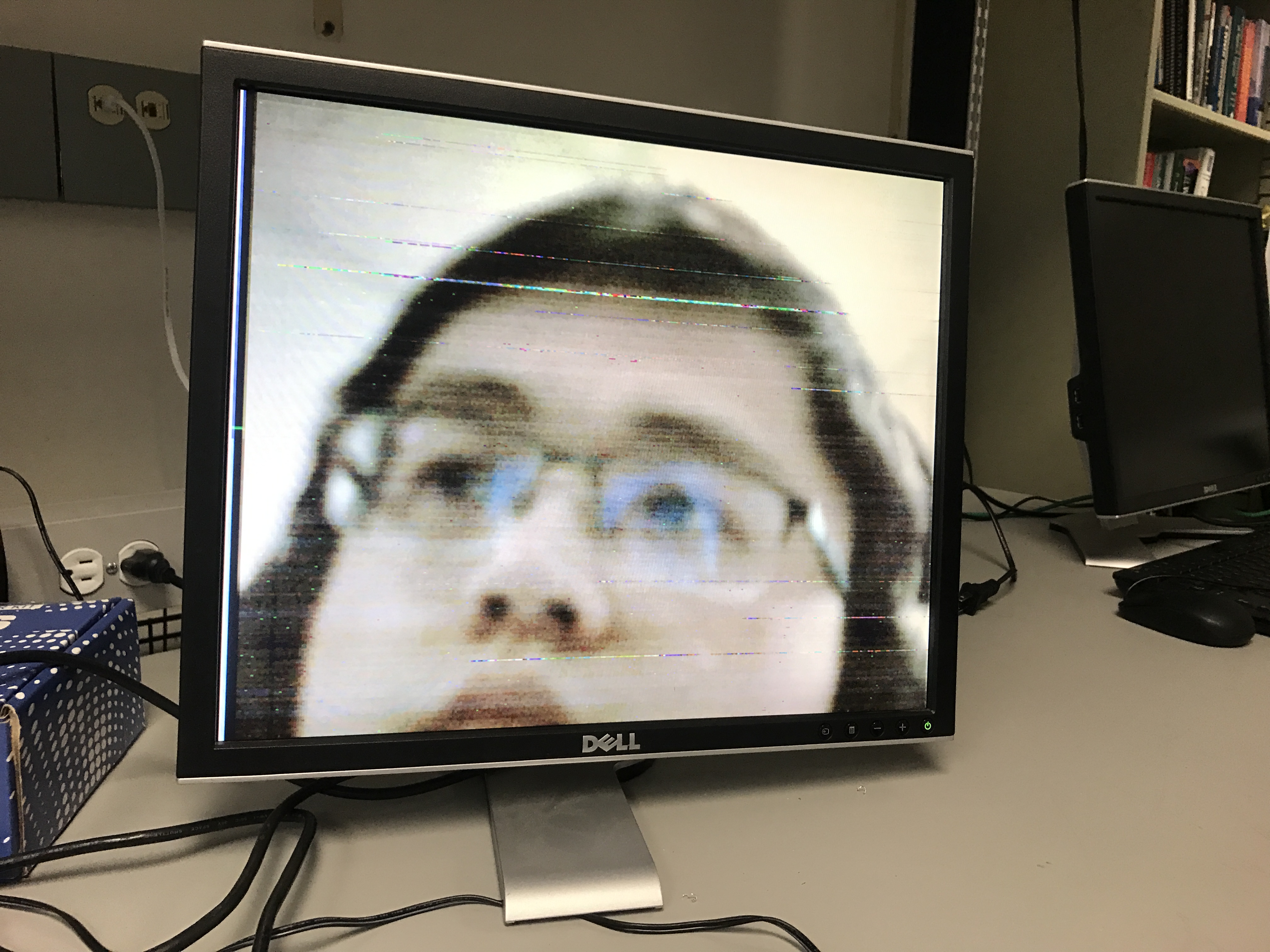
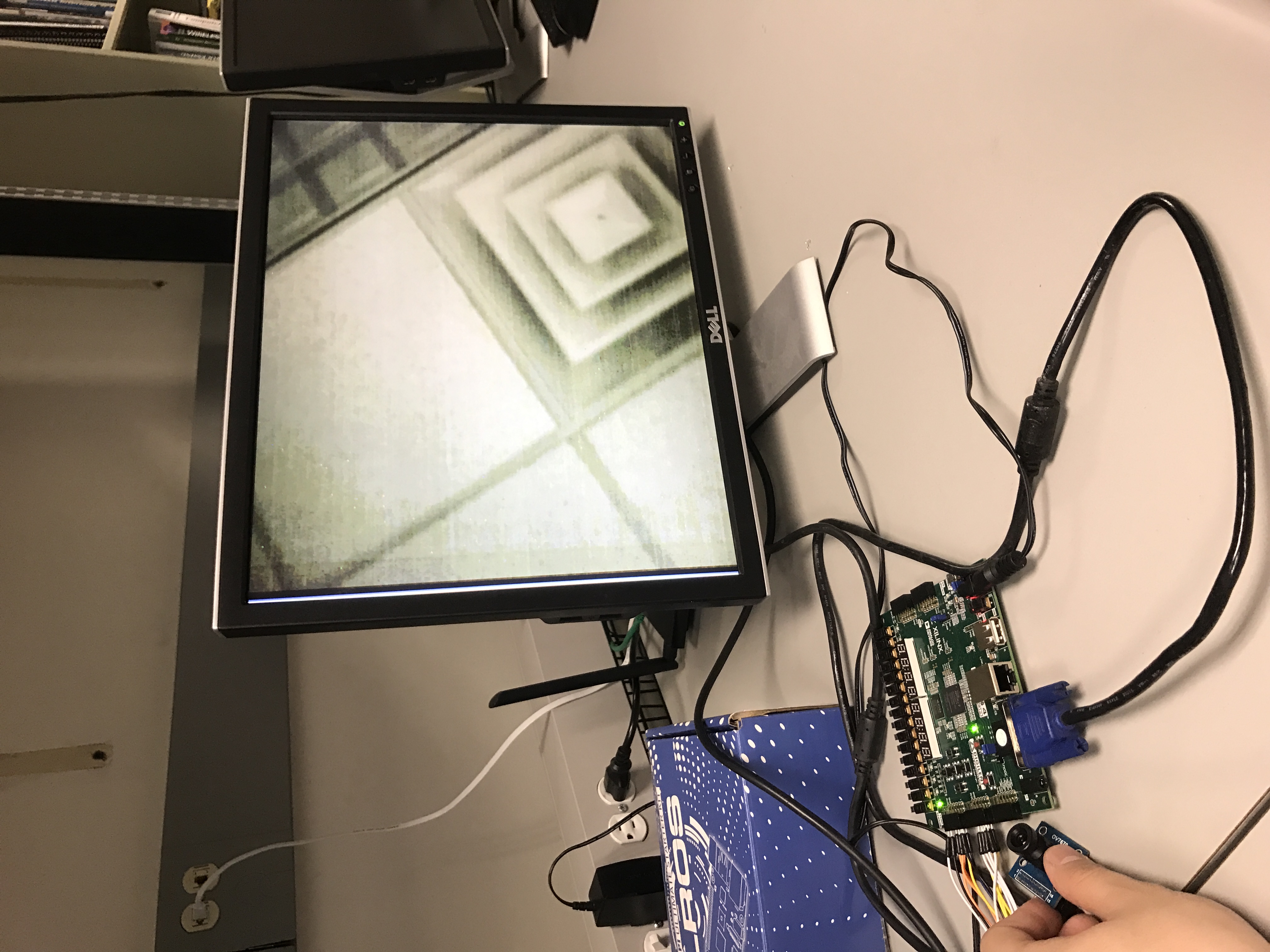
I this project, I will interface a camera module OV7670 to the nexys4DDR board. The camera module is configured using I2C interface. The register configuration is preloaded in the FPGA logic. A simple BRAM on the FPGA is used to buffer the captured video data, the buffered data will then be sent to the VGA output and displayed on the monitor.
If you want to duplicate this project on your own FPGA board, the source HDL code of this project is found from this Github Repository. This code is packed in Vivado and modified a little bit to be able to run it on Nexys4DDR board (hint: the vga output format is a little bit different).
Also, this page offered a lot of useful information when I started.
Camera Interface
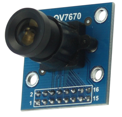
PIN |
SIG |
PIN |
SIG |
|---|---|---|---|
1 |
D1 |
2 |
D0 |
3 |
D3 |
4 |
D2 |
5 |
D5 |
6 |
D4 |
7 |
D7 |
8 |
D6 |
9 |
PCK |
10 |
XCK |
11 |
VS |
12 |
HS |
13 |
SCL |
14 |
SDA |
15 |
3V3 |
16 |
GND |