ECE429 Intro to VLSI (Fall2013)
ECE429 is a course at IIT called Introduction to VLSI Design. I took it in Fall 2013, it was the second first semester of my M.S. degree. Back in time, I was my first few month starting to work with English. The writing and understanding of the course material are still very limited. However, I learned a lot from this course of Dr. Oruklu’s. This project was done by me and a classmate of mine as a group work.
Table of Contents
Introduction
In this project, we are going to design and implement 4 different kind of adders and an additional multiplier as a bonus. They are carry ripple adder, carry select adder, carry skip adder and prefix adder. These adders have different performances. Some of them are fast and some of them cost less hardware and some of them are easy to design. After designing these adders, I am going to see the differences between these adders by implement the hardware design based on the automatically synthesis tools.
This project introduces VLSI design concepts including datapath circuit design, standard cell based design flow, and design validation and verification through construction of fast adder architectures in Verilog, to be synthesized using commercial EDA tools from Synopsys and Cadence Design Systems. The intent is to show, first, how to construct a nontrivial adder hardware; second, how to make design trade-offs, e.g. performance, cost, and design time, through architectural exploration; and third, how the EDA tools transform the design implementation from higher abstraction levels, e.g. Verilog, to lower abstraction levels, e.g. layout, through cell-based design flow, what the differences are among the implementations and how to verify their correctness at the different abstraction levels.
Background Knowledge
In the previous lab, we have implemented the 4 bit carry ripple adder in lab 7 to lab 9. The adder we design in the lab are actually carry ripple adders. The following two equations are the basic of the design.
\(S=A \oplus B \oplus C_{i n}\)
\(C_{\text {out}}=(A \cdot B)+C_{i n^{*}}(A \oplus \mathrm{B})\)
By using the Cout in the equation of the Sum, we can save the hardware during implementation.
\(s=(A+B+C) C_{o u t}+A B C\)
\(C_{\text {out}}=A B+(A+B) C_{i n}\)
There is a big problem in this implementation. That is the delay is linearly increasing with the size of the adder. So we are going to develop some new adders with less delay.
After we have learned chapter 11, we know that when add two 1 bit numbers together, we can generate three additional signals. They are Generate, Propagate and Kill as it shown in the following Table.
A |
B |
Cin |
Generate |
Propagate |
Kill |
Cout |
Sum |
0 |
0 |
0 |
0 |
0 |
1 |
0 |
0 |
0 |
0 |
1 |
0 |
0 |
1 |
0 |
1 |
0 |
1 |
0 |
0 |
1 |
0 |
0 |
1 |
0 |
1 |
1 |
0 |
1 |
0 |
1 |
0 |
1 |
0 |
0 |
0 |
1 |
0 |
0 |
1 |
1 |
0 |
1 |
0 |
1 |
0 |
1 |
0 |
1 |
1 |
0 |
1 |
0 |
0 |
1 |
0 |
1 |
1 |
1 |
1 |
0 |
0 |
1 |
1 |
When the Generate and Kill signals are set to 1, it means that the carry out bit is no longer related to the inputs. If Generate is 1, then the carry out is always 1. If the Kill is 1, then the carry out is always 0. If the Propagate signal is 1, then the carry out signal is based on the input carry in, A and B. These three signals can be obtained by using the following equations.
\(\mathrm{G}_{\mathrm{i} ; \mathrm{i}}=\mathrm{G}_{\mathrm{i} : \mathrm{k}}+\mathrm{P}_{\mathrm{i} : \mathrm{k}} * \mathrm{G}_{\mathrm{k}-1} : \mathrm{i}\)
\(\mathrm{P}_{\mathrm{i} : \mathrm{j}}=\mathrm{P}_{\mathrm{i} : \mathrm{k}} * \mathrm{P}_{\mathrm{k}-1 : j}\)
The base case can be represented as
\(\mathrm{G}_{\mathrm{ij}}=\mathrm{G}_{\mathrm{i}}=\mathrm{A}_{\mathrm{i}} * \mathrm{B}_{\mathrm{i}}\)
\(\mathrm{P}_{\mathrm{ij}}=\mathrm{P}_{\mathrm{i}}=\mathrm{A}_{\mathrm{i}} \oplus \mathrm{B}_{\mathrm{i}}\)
After the computation of PG logic, we still have to get the final Summation and the Cout. The logic are shown as the following equations.
\(\mathrm{C}_{\mathrm{out}}=\mathrm{G}_{\mathrm{N}}+\mathrm{P}_{\mathrm{N}} \mathrm{G}_{\mathrm{N}-1.0}\)
\(\mathrm{S}_{\mathrm{i}}=\mathrm{P}_{\mathrm{i}} \oplus \mathrm{G}_{\mathrm{i}-1 : 0}\)
Different adders that are based on PG logic have different performances which we will discuss it specifically later. However, adders that are based on PG logic have the same form as well.
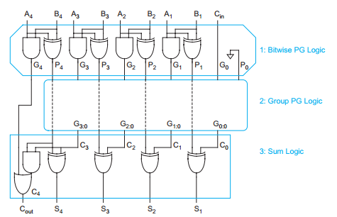
In the picture is the basic design of the adders based on the PG logic. At the first step, it computes the P and G by using the equations list before. Then the PG logic goes to a box. The box contains the group PG logic which will decide what kind of adder it is. This adder structure will be used in the prefix adder.
implementation and Simulation
Carry Ripple Adder
Design
The first adder that we are going to implement is the most basic one, carry ripple adder. The carry ripple adder is constructed by some 1 bit full adders. Each 1 bit full adder sent their output to the next one. So the delay is kind of high due to the adders have to wait for the previous adder to generate the Cout. The 1 bit full adder is realized by the following equations
\(s=(A+B+C) C_{o u t}+A B C\)
\(C_{o u t}=A B+(A+B) C_{i n}\)
The carry ripple adder group PG network can be shown in the following picture.
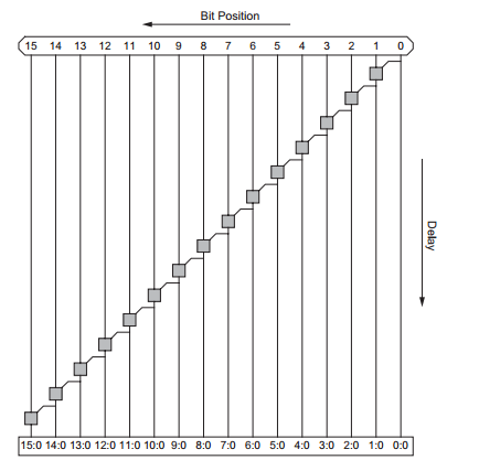
Although the one we implement in the project is not based on the PG logic. But still, it can show us the delay of the carry ripple adder. In the picture is the 16 bit carry ripple adder. As we can see in the picture, each adder has to wait their previous adder to compute the summation. The critical path delay of the carry ripple adder is
\(t_{\text {ripple}}=\mathrm{t}_{\mathrm{pg}}+(\mathrm{N}-1) \quad \mathrm{t}_{\mathrm{AO}}+\mathrm{t}_{\mathrm{xor}}\)
implementation
The implementation of the carry ripple adder is simple. Just create the 1 bit full adder module and then connect them to 4 bit full adder. Then connect two 4 bit full adders to build 8 bit full adder. The 32 bit carry ripple adder is then built up by four 8 bit carry ripple adder.
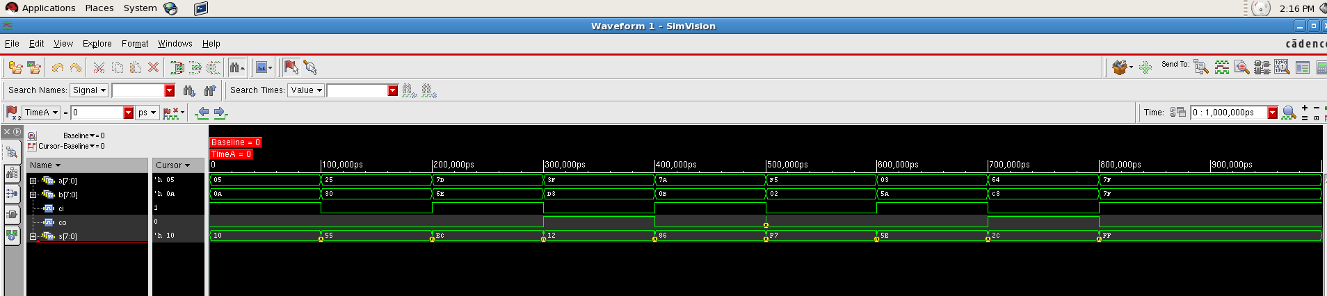
Simulation and Result
Then, we are going to simulate the carry ripple adder. There are two part of carry ripple adder, one is 8 bit carry ripple adder, one is 32 bit carry ripple adder.
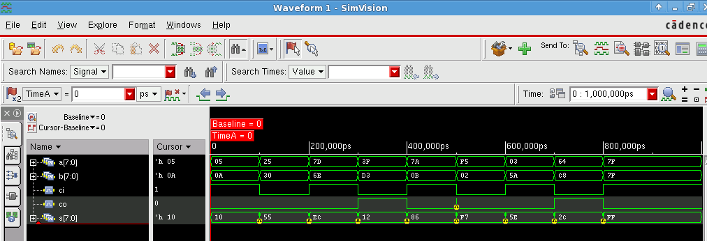
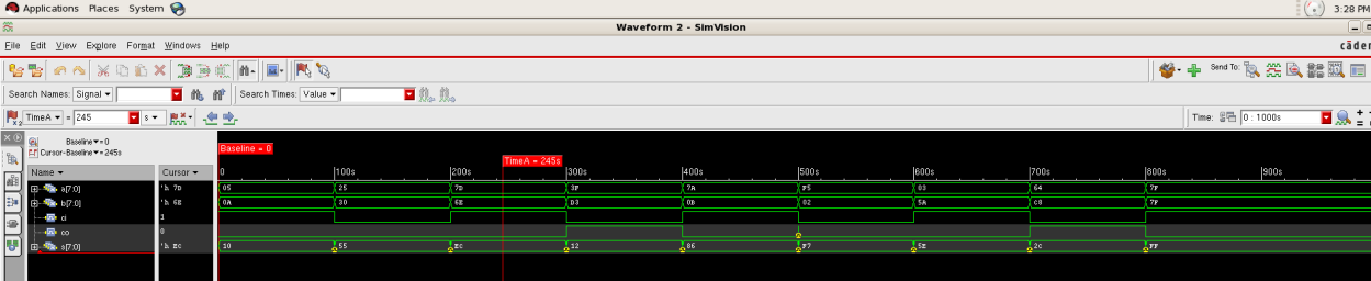
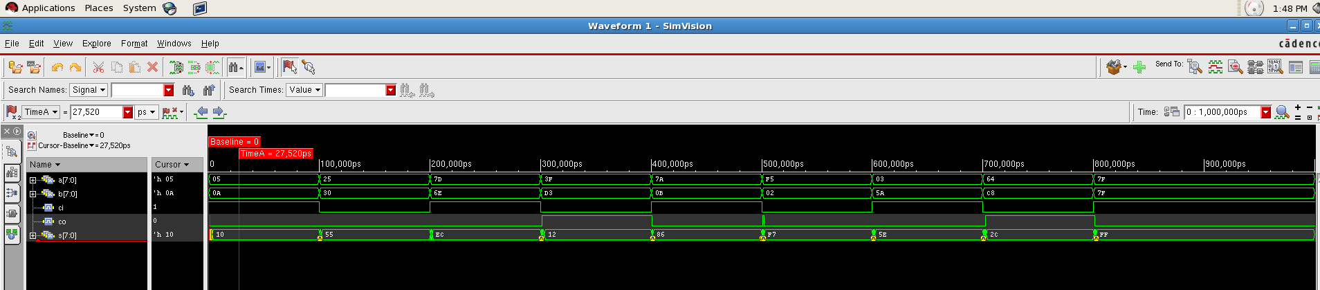
(1) 8 bit carry ripple adder
After compilation of the code, the simulation result of the behavioral level is shown in the simvision in the following picture.
Carry Skip Adder
Design
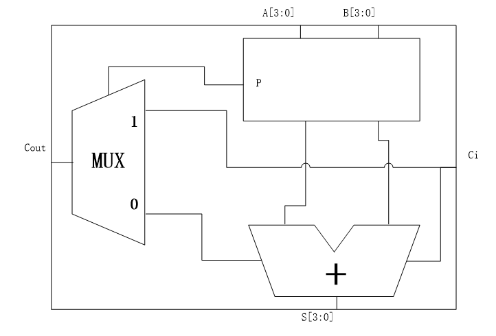
The carry skip adder design is based on the PG logic and the 4 bit carry ripple adder. The figure on the right shows the 4 bit carry skip adder.
The carry skip adder can decrease the delay by compute the logic Propagate first. As I have descripted before, when the propagate signal is 1, the carry out bit of the design will be related to the cin from the previous adder. So, carry skip adder use a multiplexer driven by p logic to choose which path to go. The Propagate signal can be obtained by the following equation of a 4 bit carry skip adder.
\(P=[A[0] \oplus B[0]] \cdot[A[1] \oplus B[1]] \cdot[A[2] \oplus B[2]] \cdot[A[3] \oplus B[3]]\)
The carry skip adder PG logic network can be shown in the following picture
The critical path delay is
\(t_{skip}=t_{pg}+2(n-1) t_{AO}+(k-1) t_{MUX}+t_{XOR}\)
Obviously, the delay of the carry skip adder is much lower than carry ripple adder.
implementation
The implementation of the carry skip adder is to connect several 4 bit carry skip adders together to get a lager adder. For example, in the following picture, is the 14 bit carry skip adder by connecting four 4 bit carry skip adders.
I am going to implement the 8 bit and 32 bit carry skip adder in the project. The procedure is no more than connecting more 4 bit carry skip adders.
I am going to implement the 8 bit and 32 bit carry skip adder in the project. The procedure is no more than connecting more 4 bit carry skip adders.

Carry Select Adder
Design
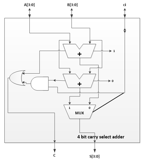
The picture on the right shows the basic block of a carry select adder. It is a four bit carry select adder. The basic design of the carry select adder is adding the input with carry in is both 0 and 1. The main delay in the adders is the delay of propagating the carry bit. With carry select adder, we have already computed the answer of carry in bit is 1 and 0. All we have to do is to select which one to use. So we name it carry select adder.
As we can see in the figure, the carry in is used to select which adder to use. In this way, we can save a lot of time by computing all the result first and using the carry in to select the correct one. The summation compute equation of the carry select adder is
\(S[i]=C_{i n} \cdot A[i]+\overline{C_{i n}} \cdot B[i]\)
The critical path delay is
\(t_{\text {select}}=t_{p g}+[n+(k-2)] t_{A O}+t_{M U X}\)
implementation
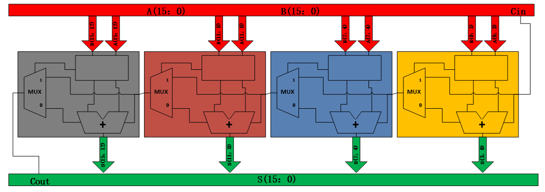
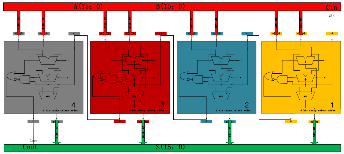
By connecting four 4 bit carry select adders together, we can get 16 bit carry select adder as follow. The 8 bit and 32 bit carry select adder is no more than changing the number of the 4 bit adder.
Prefix Adder: Koggle Stone
Design
Here comes the trickiest one. The prefix adder which name is kogge stone. There are many ways to build the prefix adder that offer trade offs among the number of stages of logic, the number of logic gates, the maximum fanout on each stage and the amount of writing between stages. The kogge stone prefix adder that we are going to implement has the critical path delay of
\(t_{\text {prefix}}=t_{p g}+\left\lceil\log _{2} N\right\rceil t_{A O}+t_{X O R}\)
This is a kind of very fast prefix adder. And the fanout of each stage is just 2. This comes at the cost of many long wires that must be routed between two stages. The prefix adder contains more PG logic which means it will cost more to build.
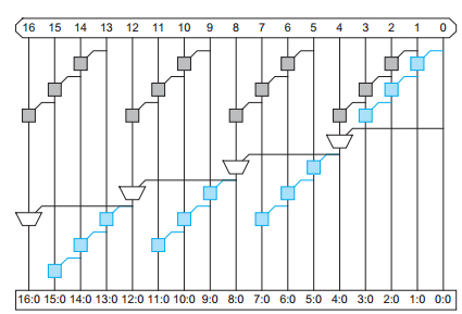
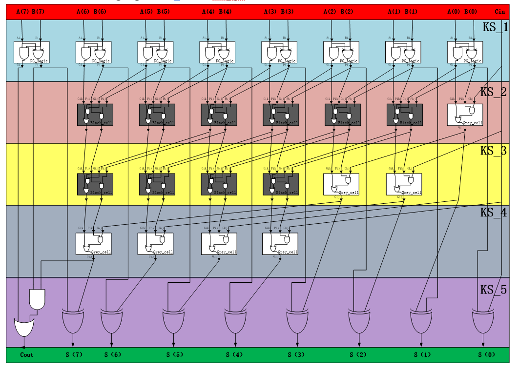
The overall PG logic network is shown in the following picture.
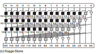
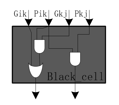
This is a 16 bit kogge stone prefix adder. There are basically two kind of blocks in the graphic. The black one is called black cell and it implements the function of:
\(\left\{\begin{array}{l}{G_{i : j}=G_{i : k}+P_{i : k} \cdot G_{k-1 : j}} \\ {P_{i : j}=P_{i : k} \cdot P_{k-1 : j}}\end{array}\right.\)
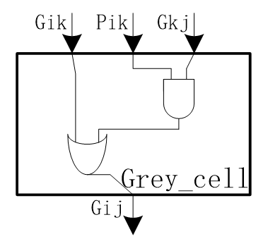
It has 4 inputs and two output. The grey one is called grey cell and it implements the function of:
\(G_{i : j}=G_{i : k}+P_{i : k} \cdot G_{k-1 : j}\)
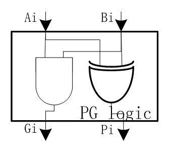
The triangle part is the buffers. And the following one is the PG logic, which is used in the first step to generate the Propagate and Generate signals.
\(\left\{\begin{array}{l}{G_{c i}=G_{i}=A_{i} \cdot B_{i}} \\ {P_{i i}=P_{i}=A_{i} \oplus B_{i}}\end{array}\right.\)
By connecting these basic block in the way it shows in the adder PG network, we can get a kogge stone prefix adder.
implementation
Here in the following figure is a 8 bit kogge stone adder.
This time, I cannot connect several low bits prefix adders to get the high bits prefix adder because that won’t show the advantages of the prefix adder.
bonus: multiplier
Design
If we are going to implement the multiplier in hardware, the first thing we are going to do is to invest what happened when multiplied two binary numbers together. In the following picture, it convert the multiply process to many add and shift processes.
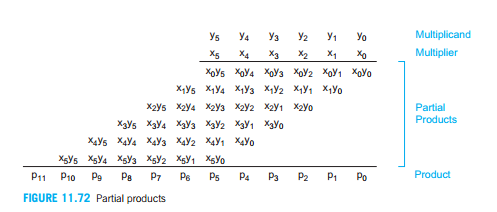
It is easy to understand that when multiply two numbers together, the biggest result length will be the addition of the multiplicand and multiplier. Take the four bit multiplier as an example.
When multiplying two 4 bit binary numbers together, we can get the maximum result of 1111*1111= 11100001 which is 8 bit. In the following picture, it shows the structure of the array multiplier of 4 bit.
The multiplicand y is multiplied by the multiplier x.
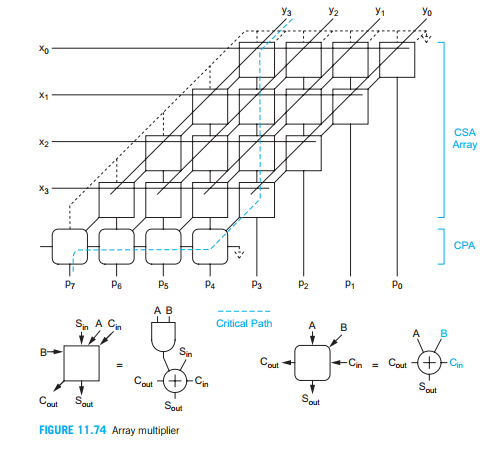
There are two kinds of blocks in the picture, one is the CSA and another one is CPA. By connecting these two kinds of blocks together, we can get the multiplier.
implementation
The block CSA can be implemented by the Verilog code as:
module csa (si,ci,a,b,so,co);
    input si,ci,a,b;
    output so,co;
    wire prod;
    assign prod=a & b;
    assign {co,so}=si+prod+ci;
endmodule
The block CPA can be implemented by the Verilog code as:
module cpa (x,y,cin,s,co);
    input x,y,cin;
    output s,co;
    assign s=x^y^cin;
    assign co=(x&y)|(x&cin)|(cin&y);
endmodule
In the top module, we are going to connecting these blocks to build a multiplier. The problem is there are 16*16 cra blocks in the 16 bit multiplier. So I am going to combine the row into a separate module. So that I can only use 16 row module in the top module. That can save me a lot of work.
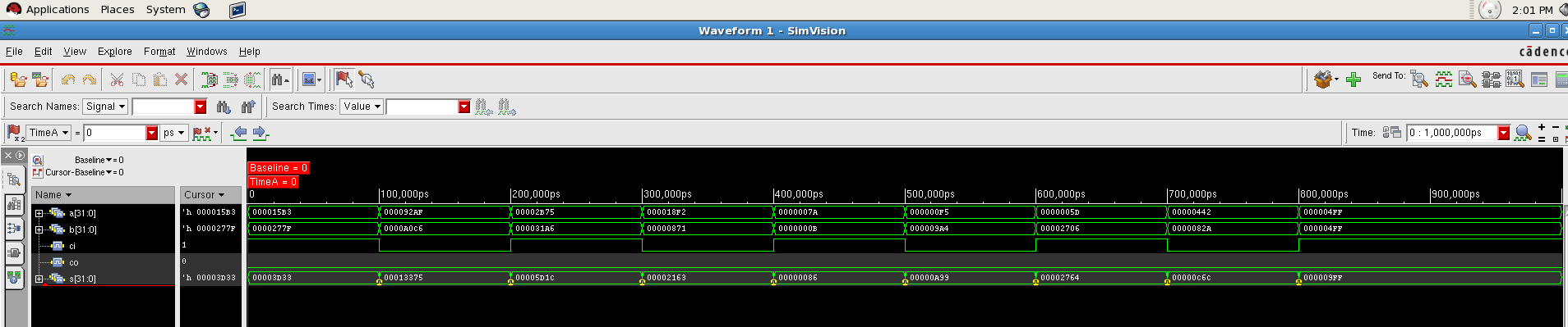
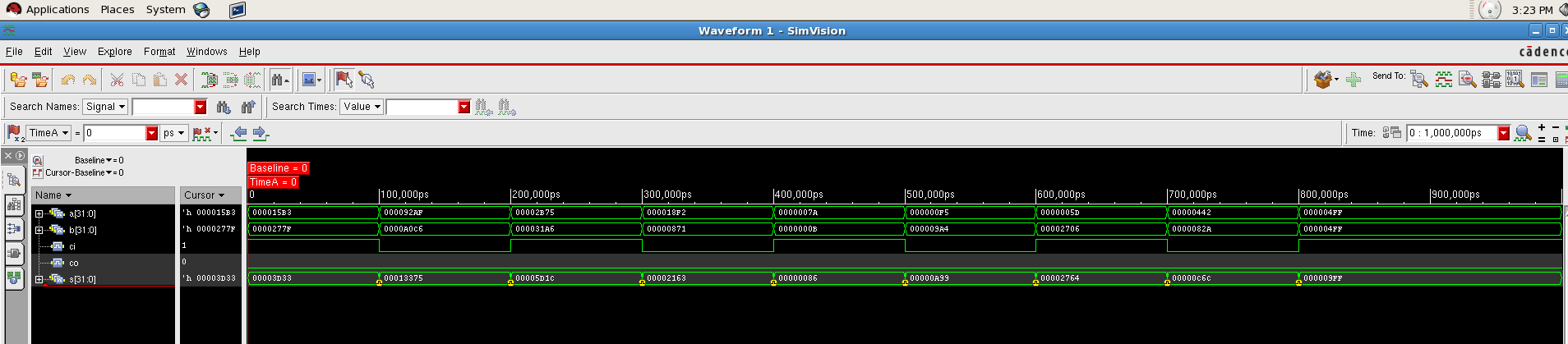
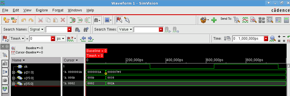
Simulation and Result
16 bit multiplier After compilation, the result is shown in the simvision as follow
Conclusion
In the project, I learned different implementation methods of adders in VLSI. This helped me get a better understand of the VLSI course.
Statement
This is a course project, all the raw data are provided by Dr. Erdal Oruklu thought course ECE429 at IIT. Please contact me if you find any problem.