ECE529 Advanced VLSI Systems Design (Spring2014)
ECE529 is a course at IIT called Advanced VLSI Systems Design. This is an advanced course of ECE429
Table of Contents
Introduction
In this project, we are going to design and implement the 5 bit multiplier using Conventional Domino Logic and Split Path Data Driven Dynamic Logic. After the implementation, the properties of these two CMOS techniques will be compared. The design of the circuit will be at transistor level to assure different techniques. We will use Cadence IC 6.1 tool for schematic entry. The circuit will be simulated and analyzed by using Synopsys Hspice. The challenges in this project are:
First, how to decide the W/L ratio of each transistor.
Second, which type of inverter should be chosen in the domino logic.
Third, how to performs the SPD3L schematic so that the logic can satisfy the D3L characteristic, the PUN will be pre-charged during pre-charge phase and PUN will not work while evaluation phase.
To overcome these challenges, we follow the specific method. First, searching the related papers. Second, based on the knowledge from previous semesters. Third, test the implementation in the virtuoso and analyze the result. Fourth, make a good communication with the professor.
Background
multiplier
To design the 5-bit array multiplier, we first should understand its architecture. As shown in Figure 1, each full-adder cell will accept one bit of new partial product , one bit of previously accumulated partial product, and carry-in bit.
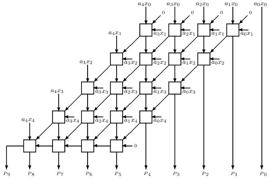
Figure 1. Array Multiplier Architecture
In the first 4 rows, there is no horizontal carry propagation accumulated partial product consists of intermediate sum and carry bits. Otherwise, last row is a ripple-carry adder which can be replaced by a fast 2-operand adder. In the way it shown in the block diagram in figure 1, we can implement the multiplier with some AND gates and full adders.
Conventional Domino Technique
Conventional CMOS Dynamic Domino circuits operate using a sequence of pre-charge and evaluation phases orchestrated by the system clock signal which shown in Figure 2.
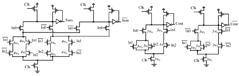
Figure 2. Full Adder Dual Rail Domino logic implementation
There are two phase during this logic working: pre-charge phase and evaluation phase. During first phase, the output signal is forced to a pre-defined value. During the evaluation phase, the output signal will change depending on the input signal. When the clock signal is low, the n-type dynamic domino circuit executes the pre-charge. Otherwise, the p-type circuit executes the pre-charge phase when clock signal is high. We have known domino gates is better than static CMOS counterparts in speed from [1]. However, domino logic may take over the noise influence through input. This is because leakage currents are flowing in the PDN (PUN) and cause an undesired discharging (charging) in the dynamic node. We often add a keeper to overcome this problem. This keeper is returning the output signal as a control signal. And it is the negative impact on the speed performances and power consumption.
However, there are some limitations in the domino logic. To overcome its logic limitation, we use dual-rail logic (D3L) to implement the inverting logic function which is recorded in [2]. It is called D3L. We can know that dynamic dual-rail domino need a clock signal to pre-set the output signals during the pre-charge phase. The D3L gate owns the characteristics as shown below[3]:
During the pre-charge phase, the PDN (PUN) is OFF, the PUN (PDN) is turned ON and the output node is charged (discharged) to Vdd (Ground);
During the evaluation phase, the output node is eventually discharged (charged) to 0 (1) by the PDN (PUN), which must be turned off.
There are two advantages of using D3L technology. First, the power consumption will be decreased by the elimination of the clock distribution network. Second, the evaluation path delay will be decreased by the elimination of the clocked NMOS (PMOS) transistor. However, the pre-charge of D3L circuits takes place through propagation path along the PUNs (PDNs) of all the cascaded gates which is different as dynamic domino logic so that the number of series-connected devices in the discharging (pre-charging) PDN (PUN) and gate input capacitances are minimized.
Split Path Data Driven Dynamic Logic
SPD3L is a new dynamic logic. The main advantage of SPD3L is it can minimize delay and energy penalties. The topic idea to split the PDN (PUN) is one for each product sub function. As the results, the delay and the energy consumptions are reduced with respect to the D3L counterpart. One more advantage is splitting of PUN (PDN) can increase the gate speed through the split of parasitic capacitance of the dynamic node. By this technology, each PUN only includes only one PMOS transistor so that the dynamic energy consumption reduced. On the other hand, if we use smaller keeper transistors, the dynamic energy consumption has a further reduction.
SPD3L also implements efficient dual-rail circuits. This characteristic can improve the gate speed and consequent energy saving.
In the third difference and improvement, SPD3L did not use clock signal. SPD3L uses a subset of input data signals for pre-charging the dynamic node, thus avoiding the clock distribution network.
The schematic of SPD3L if shown in Figure 3
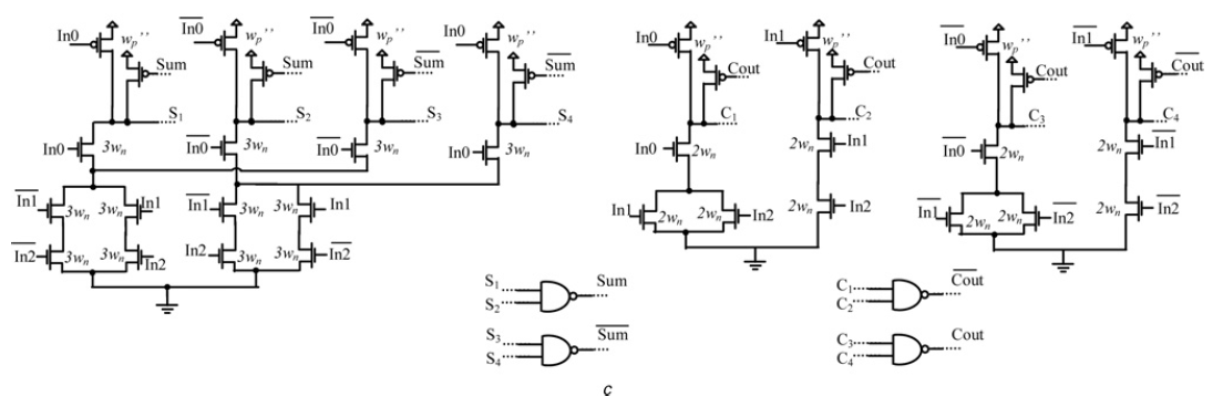
Figure 3. Split-Path Data Driven Dynamic Logic implementation of the Full-Adder
Beside, we should be careful in the SPD3L pre-charge phase. We have known that In0 signal make the PUN and PDN only one part work. It is easy to achieve if there is just one logic, one bit calculation. In this technique, the original pull down logic is split into two parts. And one more pull up transistor is added to the logic. The control signal of the pull up memory is one of the input of the pull down memory. In this way, there are two pull down and pull up logics to get one output or output bar. There is a possibility that one specific input will close the pull down logic. In this way, the output of the logic will be floating at the evaluation phase. So that the output will be decide by the previous status. This is definitely undesirable. So we add one more signal called pre-charge signal in our project. This pre-charge signal is AND with each control signal of the pull up logic. This signal after the and gate will be sent back to where it should go. This will make sure that after one bit computing, the output node will be pre-charged back to 1 again. During the pre-charge phase, the output will be 0 due to the NAND gate.
Architecture Exploration
The dilemma of this project is the trade-off between speed and power consumption. An accurate transistor sizing is necessary to balance the contrasting performances: delay, energy and area. If we size the transistors large, the pre-charge and discharge will be faster due to the low register of the transistors. However, it will increase the power consumption of the whole system. This is also due to the low register transistors. If we size the transistors small, the logic will be slower, but the power performance of the system will be better though. The best thing is to find a best number of wn which will gives us both the best power consumption performance and the lowest delay.
The size of the pull up transistors are set to wn. The size of the pull down transistors is decided by the numbers of the transistors in series. Take the COUT logic as an example, the discharge path has 3 transistors, to ensure the same skew of the positive edge and negative edge, we size it to 3wn. Same thing for the pull down transistors in the SUM logic, the pull down transistors are sized to 4wn. In the SPD3L, the pull down transistors is sized as 2wn in COUT logic. In SUM logic, NMOS are sized as 3wn.
In our design, wn is set to 90nm. This may not be the best choice in our design of multiplier. But with all the wn set as 90 nm, I can still make a comparison in all these implementations.
In the implementation of the domino logic, we adopt high skew inverter to favor the positive edges in the output. This is due to the Domino logic will not have a negative edge during the evaluation phase.
Function Validation and Verification
In this section, I am going to shows the full adder design procedure and simulation result of each technique.
Dual rail DOMINO adder design
Dual rail DOMINO AND gate design
As I have mentioned in the multiplier implementation method, the multipliers are implemented by using adders and AND gates. So the first procedure is to design an AND gate. Due to the logic is applied using DOMINO technique. The DOMINO technique has a pitfall that the output is not able to vary from 1 to 0 during the evaluation phase. So the DOMINO gate has to be driven by another DOMINO gate. So I design a Dual rail DOMINO AND gate here to optimize the design.
The schematic of Dual rail DOMINO AND gate can be shown in the left figure. As it shown in the schematic, there are two outputs there, one is a AND b, another one is a NAND b. This gives us both output and output bar. It can also ensure the logic diversity here. One more advantage of this circuit than using one NAND gate and one inverter is the delay of output and output bar of this circuit is the same. The design with NAND gate and INVERTER will gives us different delay at output and output bar. Different delay at the input gate will cause glitches at the output.
High skew inverter design
In the DOMINO circuit, there is one important thing is that the inverter before the output is a high skew inverter. High skew inverter favors the positive edge of the output. It can be implemented by sizing the pull up transistor larger. The following figure shows the simulation waveform of the high skew inverter. The PMOS is sized as 4wn. The NMOS is sized as wn.
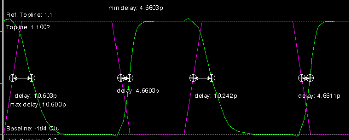
The delay of the positive edge is 4.6603p and the delay of the negative edge is 10.603p. It has a significant improvement of the up edge delay and there is a penalty at the down edge. This is exactly what we want in the DOMINO logic because there will be no down edge at the evaluation phase.
SUM logic Design
We have designed the full adder for several times in the previous study life. The logic of SUM is
\(S=A \oplus B \oplus C_{i n}\)
After simplification, this logic can be implemented by using the following schematic.
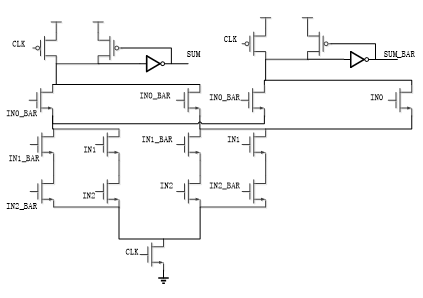
As we can see in the schematic, it is a Dual rail DOMINO design implementation. Both input and input bar are needed as inputs. Both footer and header transistors are used to eliminate additional static power consumption. It means that during the pre-charge phase, the pull down logic will be terminated due to the footer. The inverter used in the schematic is designed as a high skew inverter to favor the rising edge of the output.
Cout Logic Design
The logic equation of the COUT is shown as follow.
\(Cout =(A \cdot B)+C_{i n^{*}}(A \oplus \mathrm{B})\)
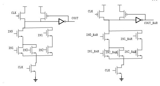
The figure on the left shows the schematic of the COUT design after implementation. It is also designed in Dual rail DOMINO technique. The COUT and the SUM are the basic components of the Full adder.
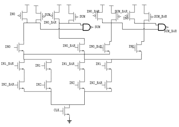
Full Adder Design
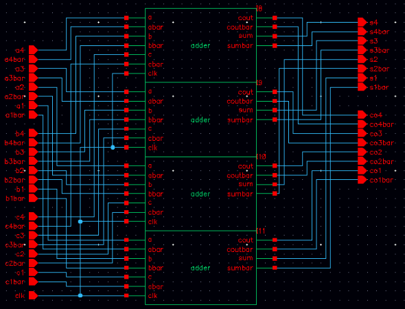
Since we already have the COUT and SUM components, the full adder can be easily implemented by connecting these two parts together as it shown in the following figure.
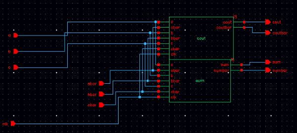
As we can see in the figure, the adder has 7 inputs and 4 outputs. One of the input is CLK signal to rhythm the DOMINO circuit. The others are input and input bar. The output is also divided into output and output bar. In this way the output of one adder can drive next dual rail domino logic.
The design of the adder is simulated by using Hspice and the waveform of the adder can be shown in the following figure.
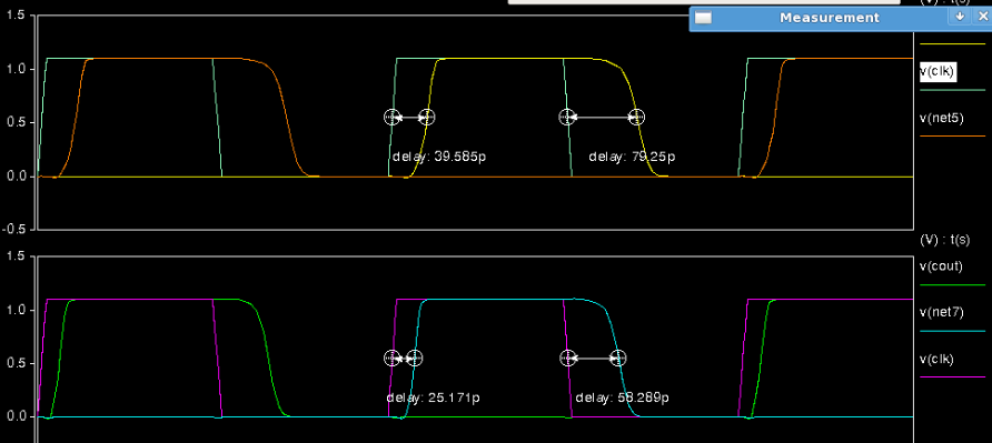
The upper one is the SUM wave form, the delay of the evaluation phase is 39.585 ps and the delay of the pre-charge phase is 79.25 ps. This can be easily explained, the PMOS which is the pull up logic is sized as W. The register is very large for this size. The pull down transistors are sized as 4 W. In this way the delay of the pre-charge phase will be twice as the evaluation phase theoretically. This is exactly what it shows in the waveform. The COUT has its evaluation delay as 27.171 ps and pre-charge delay as 58.289 ps.
Input Generator
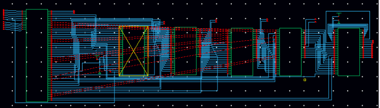
In the 5 bit multiplier, there are 25 AND gates and 20 Full adders are needed. If we draw all the components in one figure without layer division, the schematic will be a mess and extremely hard to debug. So I pack 25 AND gates together as an input generator. The schematic of the input generator is shown in the following figure.
It has 11 inputs, they are x(0) to x(4), a(0) to a(4) and CLK signal. There are 50 outputs which are NAND output and AND output.
TAP
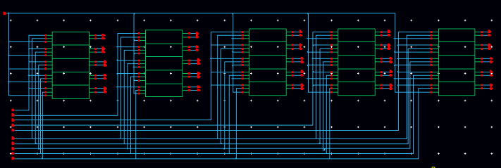
I also pack 4 adders in a line to form a TAP. The whole multiplier contains 5 TAP. The schematic of a TAP can be shown in the figure on the left side. These 4 adders are not connected with each other. The only usage of this component is to simplify the structure of the final multiplier.
multiplier
The multiplier contains 5 TAPs and 1 input generator. The structure of the multiplier can be shown in the following figure.
The red wires in the figure are also useful wires. The reason that they are red is that there are no automatically path for them to pass through. So a direct red line is assigned by the Virtuoso. The largest component on the left side is input generator and the rest of the components are TAPs. The result of the multiplier can be shown in the following waveform. In this situation, the inputs here are 00111 and 10101. If the wave shown in the waveform is p*bar, then it means that p* is 0 and vice versa. The result in the figure is 0000111111. The result is completely correct.
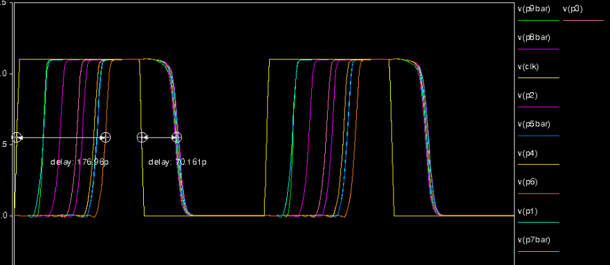
The performance including power and delay will be analyzed in the following sector.
Split Path Data Driven Dynamic Logic
SUM logic design
The figure on the left side shows the schematic of SUM logic of adder using the SPD3L technique. The difference of this logic is that there are two pull up transistors at each side of the circuit. And the pull down logic is basically the same as DOMINO logic. The difference is that the pull down logic is split into two parts. Each part will have its own pull up transistor and keeper. The missing wire is replaced by a NAND gate. Normally, the wire in the circuit can do the AND operation, it called wire and. In the DOMINO there is a inverter before the output. That’s how this technique works.
COUT logic design

This is the COUT logic implemented by using the SPD3L technique. The design procedure is basically the same as SUM logic.
We should know that only one PMOS is required to pre-charge each evaluation sub-network. As the result, the energy saving and gate speed up.
The two static output COUT and COUT_BAR inverters of dual-rail domino are also replaced by two static NAND gate.
Full Adder Circuit Design
The wire connection of the rest of the circuit is basically the same with DOMINO logic. The only difference is that the CLK signal is replaced by a pre-charge signal called PCG. The following figure shows the simulation waveform of the SPD3L adder.
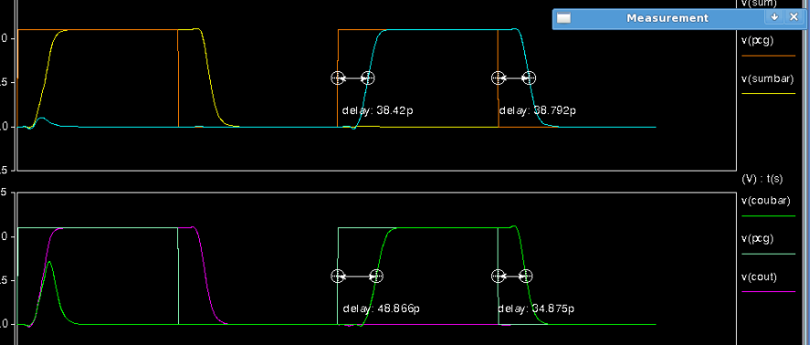
The upper one is the waveform of SUM operation. The delay of evaluation is 38.42 and the delay of the pre-charge is 38.792. This is because two pull up transistors are used in the circuit. It significantly improves the speed of the pre-charge phase.
Multiplier Design
Again, the wire connection of the multiplier is the same. Here is the simulation waveform of the multiplier.
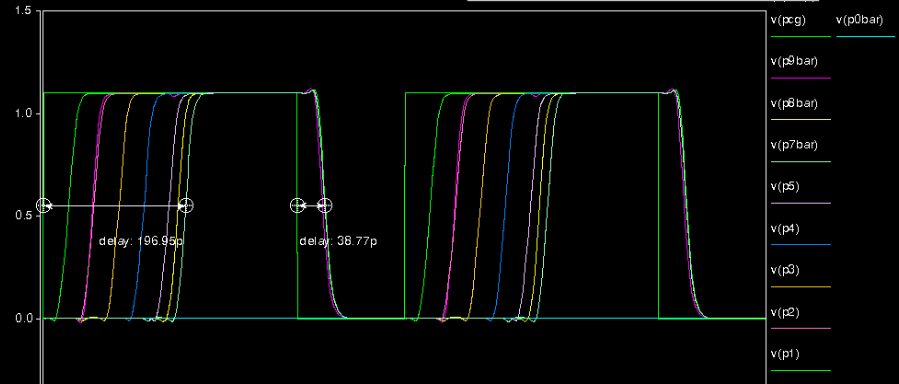
This shows that the delay of the multiplier is 196 ps in evaluation phase. The delay of the pre-charge phase is very small which is 38.77 ps.
To verify our design, we modify the .sp file for each test circuit so that we can see the input and output signals in the cscope. Then by measuring 50% of rising edge and falling edge, we can know the delay of each design. All output waveforms are listed in the appendix.
In details, we have four phases to validate and verify:
- Phase 1: Using virtuoso to build schematic
We use hierarchical design entry to create symbols for each gate.
- Phase 2: Using analog design environment (ADE-L) to simulate
In the phase, we should first build the test circuit. Then, we choose HSPICE for simulation tool and set the simulation parameters. Here, in our group, we set the total period for one cycle is 500ps with 1ps as each step.
- Phase 3: Using HSPICE to analysis power consumption
In the sp files, we need to edit the spice netlist and add following lines so that we can obtain the power results:
.PRINT TRAN POWER
.MEASURE TRAN avgpwr AVG POWER FROM 0 TO 250E-12
.MEASURE TRAN maxpwr MAX POWER FROM 0 TO 250E-12
- Phase 4: Using CSCOPE to analysis delay situation
By adding + POST command in the sp files, we can read the input, output, clock, precharge curve in the cscope which can measure delay time directly.
Bonus
For the Bonus part, I applied power gating to both design to decrease the power consumption. One more control signal called sleep signal is used here to put the system into sleep mode. In the sleep mode, the pull up network is shut down. Only static power which is leakage exists during sleep mode. High Vt transistors are used here to further reduce the leakage power consumption. During the sleep mode, if the pull down network is also shut down due to the specific inputs. The output will be floating. This is undesired. So, one single sleep NMOS transistor is used to force the output node 0. This can increase the system robustness. Next I will talk about the implementation method of the power gating of these two designs.
Power gating of the Dual rail DOMINO design
Full ADDER circuit design
The following figure shows the schematic design of the DOMINO adder after power gating
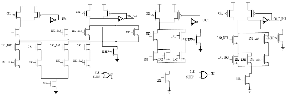
On the left side is the SUM logic after power gating and on the right side is the COUT logic. The high Vt transistors are marked with dark line. The inverter of the design has its NMOS to be the high Vt. At the input side, the clock is doing the OR operation with the sleep signal. If the sleep is 1, then the clock is forced to 1. In this way, the pull up transistor will be closed. There is a sleep NMOS transistor to discharge the output node before the inverter. During the sleep phase, the transistors still have leakage. The leakage can be reduced by using the high Vt transistors. The OR gate at the first step is also has it transistors transferred to high Vt. The other design of the power gating system is basically same with the previous design.
The power and delay performance of the system after power gating will be analyzed in the following sector.
Power gating of the Split Path Data Driven Dynamic Logic design
Full ADDER circuit design
The following figure shows the schematic design of the SPD3L COUT logic after power gating
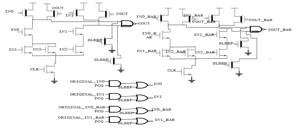
Figure 4. Power Gating implement in SPD3L COUT
The high Vt transistors are marked with black line. Two sleep NMOS transistors are used in each output. For each input of the pull up network, we have to do the OR operation with the sleep transistor. The and gate in the design is already been described in the previous SPD3L circuit design. As we can see in the figure, 4 more or gate and 4 more sleep NMOS transistors are used in the design. This is not worth it if the power consumption cannot decrease significantly.
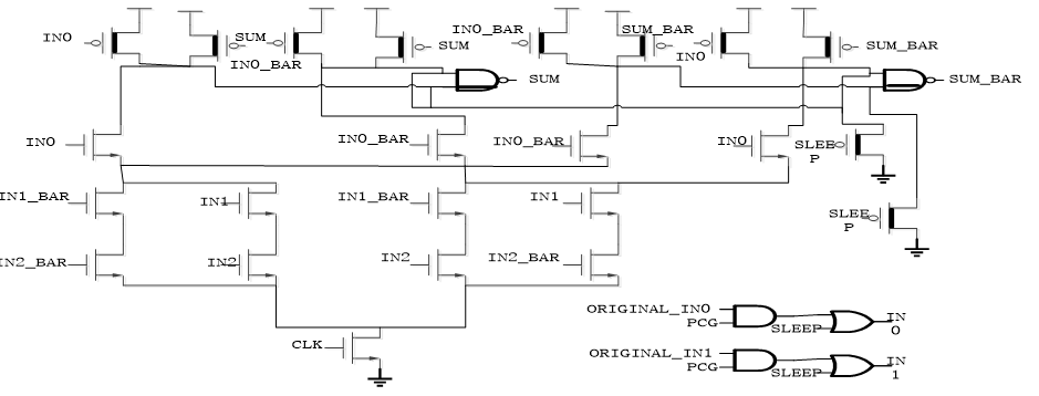
Figure 5. Power Gating implement in SPD3L SUM
This figure shows the schematic of the SUM logic using SPD3L technique after power gating. The same problem exists here. Many additional transistors are used. We will see the final performance of this design in next sector.
Comparison of these two designs
Under the same operation, we can get the power and delay data of power gate implemented in the domino and SPD3L.
Table 1. Comparison of Two Designs
Dual Rail Domino Logic |
SPD3L |
|
Dynamic Power (AVG) |
1.58e-3 |
1.96e-3 |
Static Power (AVG) |
1.64e-5 |
1.15e-5 |
Delay (Eval)/ps |
133.79 |
241.84 |
Delay (Pre-charge)/ps |
186.61 |
209.98 |
In this chart shows the comparison of the two designs after the power gating. In this sector I will only made the comparison between these two implementations. As for the comparison of the power gating system with the non-power gating system, it will be compared in the result section.
The Dynamic power consumption of the Dual rail DOMINO logic system after power gating is actually smaller than the other one. It is because that many more OR gates and AND gates are applied in the SPD3L power gating system. These transistors will consume power during the working phase. So it will consume more power. The static power consumption is measured when the sleep signal is set to 1 and the precharge signal is terminated by sleep signal. The static power consumption of the SPD3L power gating system is indeed smaller. However, compare to the additional transistors it uses, it is not a big deal.
Both the evaluation and precharge delay of the SPD3L power gating system are larger than the other one. This is also due to the additional OR and AND gate. This will cause the critical path longer. The increase of critical path will finally increase the delay of the design. This result shows that the SPD3L is not fit for the usage of the sleep signal.
So I revised the power gating system by only transform some specific transistors to high Vt transistors. This is actually gives us better performance. The sleep signal is not used in the revised power gating SPD3L circuit. The related transistors are set as high Vt transistors. The following chart shows the new power consumption information.
Table 2. Power and Delay of SPD3L implement power gating
SPD3L (Revised PWR Gating) |
|
Dynamic Power (AVG) |
7.997e-4 |
Static Power (AVG) |
1.5559e-5 |
Delay (Eval)/ps |
198.14 |
Delay (Pre-charge)/ps |
39.838 |
Results
Our objective is to compare performance of theses implementations with respect to area, delay and power.
Through schematic, we can find this two logic use different number of transistor. The conventional Dual Rail Domino uses less transistors than the SPD3L do, because additional pull up transistors, AND gate for precharge signal and NAND gate for output is used.
In Table 3 is the delay and power performance of all the designs including power gating implementation. The Dynamic power consumption is measured when the clock is set as pulse and the system is at the working status. The static power consumption of the system without power gating is to set the CLK or PCG signal to 1.1 V to close the pull up transistors. The delay is measured with the longest delay it has in all the output.
Table 3. Power and Delay Analysis of Domino and SPD3L
Dual Rail Domino Logic |
SPD3L |
Dual Rail Domino Logic PWR Gate |
SPD3L PWR Gate |
|
Dynamic Power (AVG) |
1.25e-3 |
9.84e-4 |
1.58e-3 |
1.96e-3 |
Static Power (AVG) |
5.71e-5 |
1.56e-5 |
1.64e-5 |
1.15e-5 |
Delay (Eval)/ps |
176.96 |
196.95 |
133.79 |
241.84 |
Delay (Pre-charge)/ps |
70.16 |
38.77 |
186.61 |
209.98 |
By compare the non-power gating designs, we can found that the SPD3L has the better performance at the power consumption. It has the lower Dynamic power and Static power. For the delay parameters, the DOMINO implementation has the better evaluation delay. The reason of this is because the SPD3L has a NAND gate before the output. The NAND gate has a larger delay than a single inverter do. But the difference is actually very small. The Delay of the pre-charge phase of the SPD3L technique is almost half of the other one. This is because that the SPD3L has one more pull up transistor. According to the delay difference, we actually can design a PWM wave as a PCG or CLK signal.
Compared the power gating DOMINO system with the non-power gating DOMINO system, the dynamic power consumption is slightly increased. However, the static power consumption is significantly decreased. This is exactly what this technique can assure us. As for the delay of these two implementations, for some unknown reasons, the delay in the evaluation phase of the power gating system is smaller than the non-power gating one. This shouldn’t happen. Because I didn’t change anything in the pull down logic except for one sleep transistor. It is closed during the working phase. Anyway, this is what the result shows us. We should respect the experiment result. The delay of the precharge phase is increased significantly. This can be explained by the usage of the high Vt transistors.
At last the SPD3L, non-power gating system has larger dynamic power consumption than the non-power gating system. It has a little bit smaller static power consumption than the non-power gating system. What’s more, both the delay in evaluation phase and precharge phase are larger than the non-power gating system. Compare to the delay and area and the dynamic power consumption with the slightly reduced static power consumption, we can draw a conclusion that this design doesn’t fit for the sleep signal. Actually, the PCG is already can be used to put the system into sleep mode. Just set the PCG to 1.1 V. The pull up transistors will be shut down and the system will be put into sleep mode.
Conclusion and Future Work
Through the whole project, I found that the DOMINO will have fewer transistors during the implementation. The delay performance is actually better than the SPD3L technique. The SPD3L circuit has a better performance at the power consumption. The static and the dynamic power consumption are better than the DOMINO circuit. Moreover, I applied power gating to these two techniques. The DOMINO technique fit the power gating technique I used in the project better. The dynamic power consumption is increased, but we don’t care the dynamic power of the power gating system. The static power which is the leakage is improved significantly. The delay is increased too in the power gating system. The SPD3L after power gating will take a lot more hardware. So it will bring more delay and power consumption. Although the static power consumption is less than before, but compare to the hardware incensement and delay incensement, this is actually not a good design. So I cancel the usage of the sleep signal in the power gating SPD3L. It actually gives us better performance.
In the future work, we can improve the design by looking for a best Wn size to make the best trade-off between delay term and power consumption. Also the last TAP in the multiplier can be replaced by a Carry look ahead adder instead of a Carry propagate adder.
Reference
Shepard, K.L. and V. Narayanan. Noise in deep submicron digital design. in Proceedings of the 1996 IEEE/ACM international conference on Computer-aided design. 1997. IEEE Computer Society.
Ng, P., et al., Performance of CMOS differential circuits. Solid-State Circuits, IEEE Journal of, 1996. 31(6): pp. 841-846.
Frustaci, F., et al., Low-power split-path data-driven dynamic logic. IET circuits, devices & systems, 2009. 3(6): pp. 303-312.
Statement
This is a course project, all the raw data are provided by Dr. Erdal Oruklu thought course ECE529 at IIT. Please contact me if you find any problem.